22.11.2023
Entwicklung von Diamantschichten nach Maß
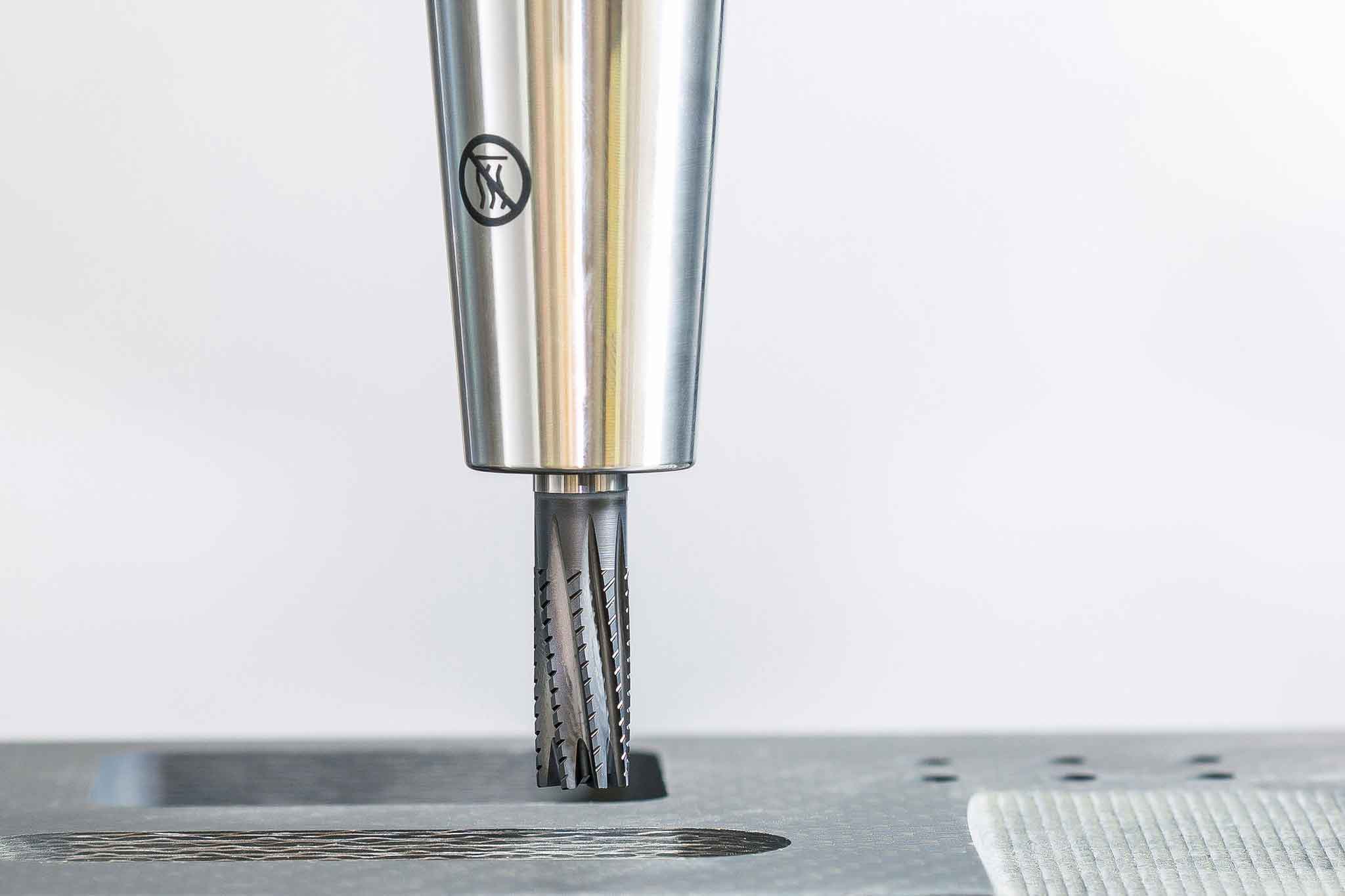
Mit seinem fundierten Know-how im Bereich der Beschichtungstechnologie entwickelt MAPAL auch extrem harte und verschleißbeständige Diamantschichten zur Zerspanung von Materialien wie CFK, Keramik, Graphit und Aluminiumlegierungen. Vor allem für Anwendungen in der Automobil- und Luftfahrtindustrie, im Werkzeug- und Formenbau und in der Medizintechnik erreichen die Zerspanungslösungen von MAPAL damit höhere Standzeiten und mehr Prozesssicherheit.
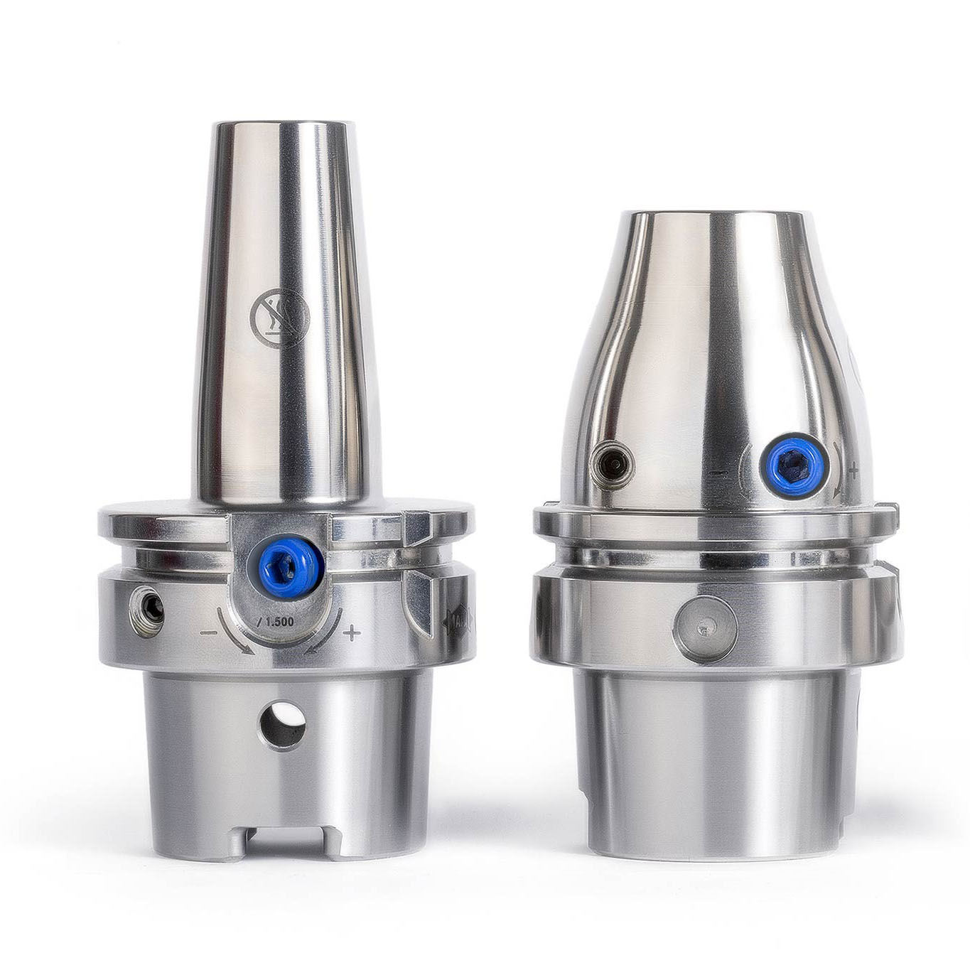
The tool manufacturer has coating technologies at its site in Aalen and in its centres of competence to coat indexable inserts and solid carbide tools using PVD or CVD processes. The choice of process depends on the relevant application parameters. For dry machining and high cutting speeds, CVD is usually chosen; in the case of unstable machining situations or difficult machining conditions, the tougher PVD coatings are applied.
If adhesive wear processes occur frequently when machining, the use of diamond-like carbon coatings (DLC) is advisable. DLC coatings are also deposited using PVD or a plasma-enhanced CVD process. These coatings are formed by a mixture of sp2 hybridised carbon atom bonds (graphite) and those with sp3 hybridisation (diamond). The mixing ratio determines the physical and mechanical properties of the coatings. The more sp3 atomic bonds there are, the harder the coating.
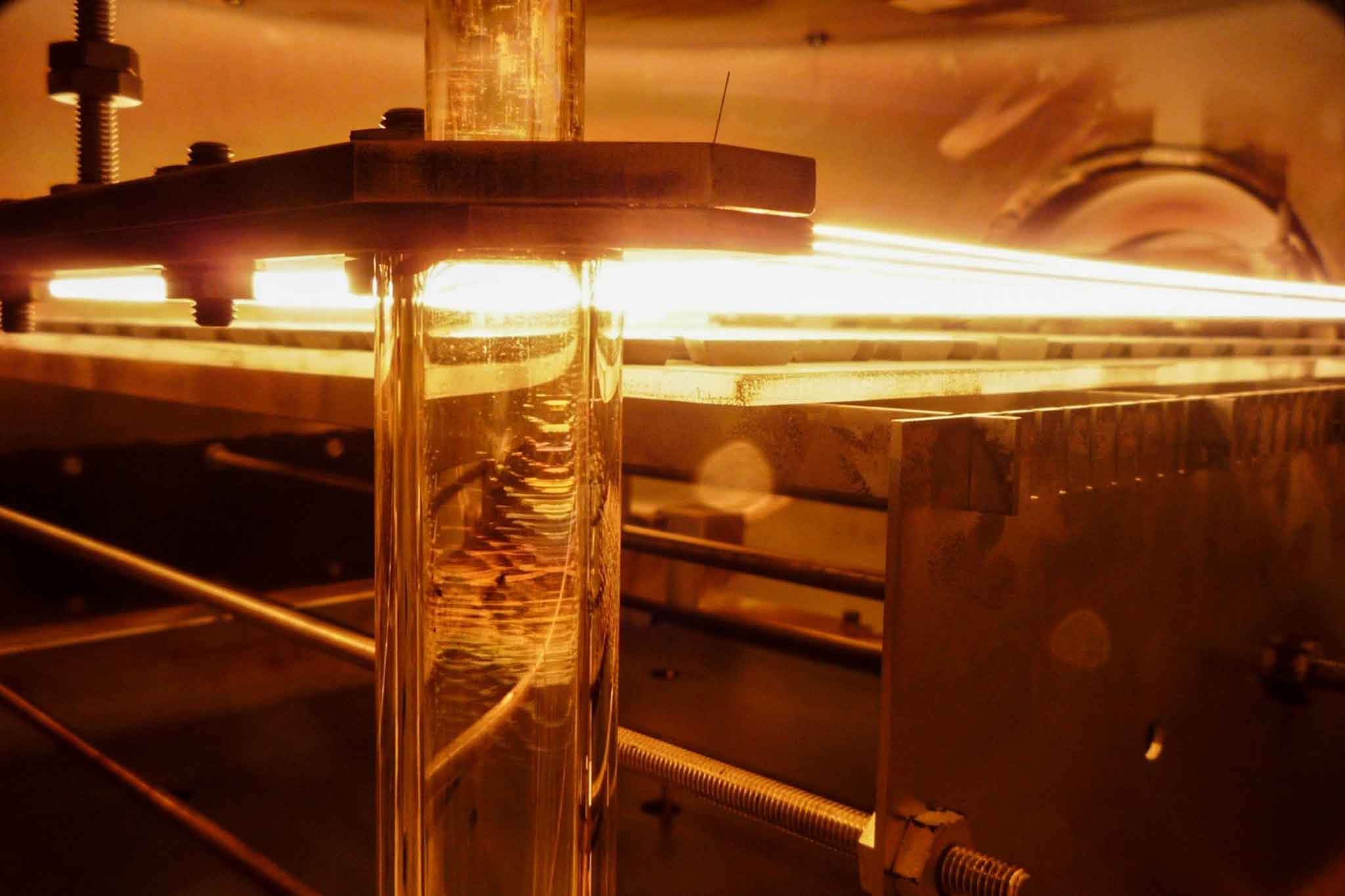
New coating processes thanks to CVD diamond reactors
“In recent years, we have worked extensively on improving the diamond coating process and have created new possibilities for MAPAL in tool production”, explains Dr Martin Kommer, Team Leader R&D Cutting Material / Coating at MAPAL. The tool manufacturer now has the complete tool design under its own control, from the appropriate geometry to the selection of a suitable carbide to the coating. This means that tools can be designed even more precisely to meet customers’ requirements. The development department in Aalen has its own centre for machining, which tests new tools for tool life and wear behaviour, among other things.
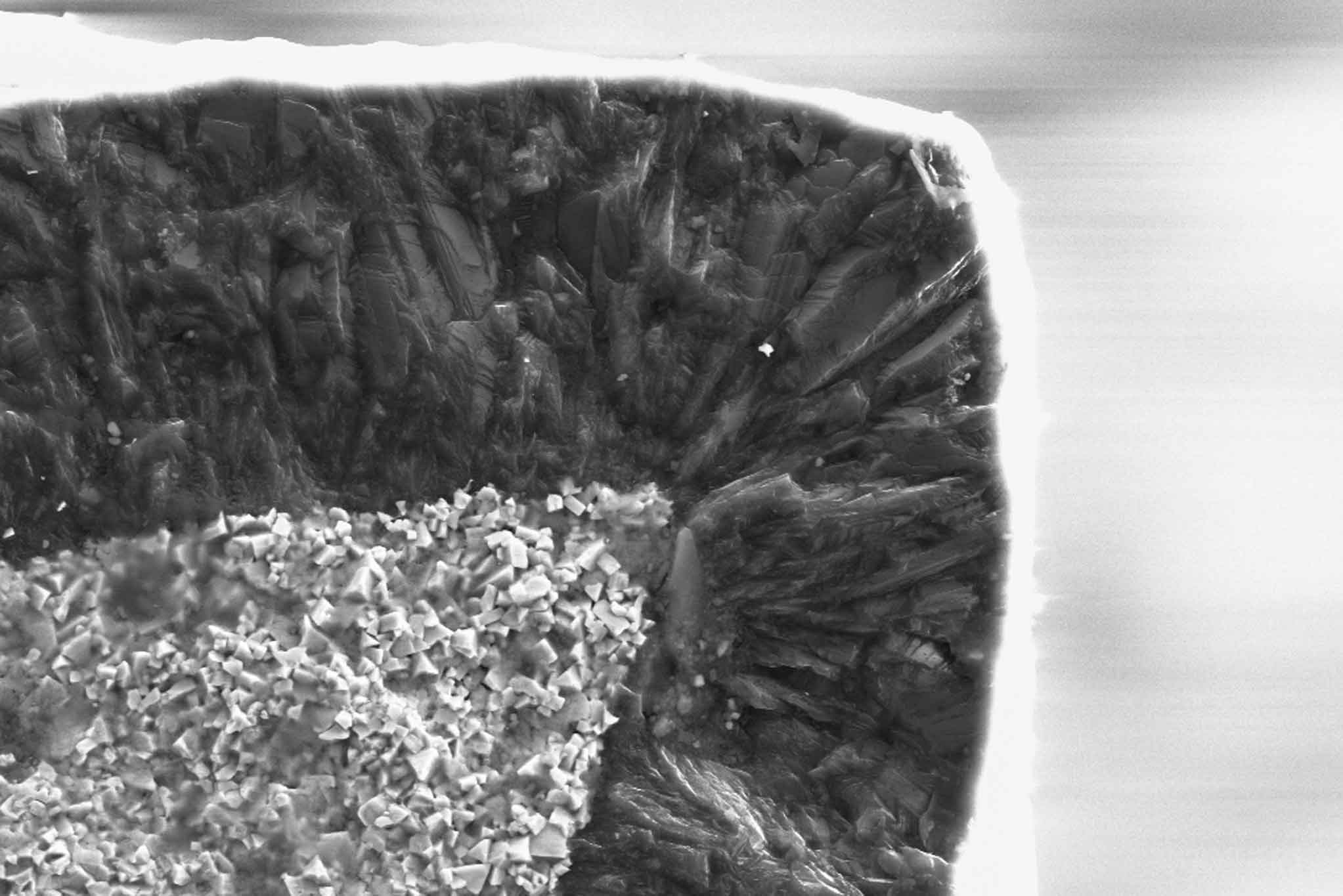
Since the coating process functions via a chemical reaction combined with mechanical clamping, defined etching of the carbide surface and seeding are important during pre-treatment. As not every carbide is suitable for this, MAPAL evaluates appropriate substrates. Whether fine-grained microcrystalline or nanocrystalline layers are produced during coating is determined by the temperature, pressure and flow of the respective reactive gases during the process. Theoretically, layers up to a thickness of 50 µm can be produced by HF-CVD. For coating its tools, MAPAL currently focuses on the range between 3 µm and 15 µm, depending on the respective application.

Contact
Kathrin Rehor Public Relations Kathrin.Rehor@mapal.com Phone: +49 7361 585 3342


